
Working With Prototype PCB Assembly
Prototype PCB assembly is a crucial step in developing new electronic devices. The process enables designers to test functionality and identify errors in design prior to manufacturing. This helps reduce costs associated with rework and production delays. However, there are several challenges associated with working with prototype pcb assembly that must be overcome.
The first challenge involves selecting the right manufacturer for prototype PCBs. It is important to choose a manufacturer with the experience and expertise necessary for your project. Experienced manufacturers are more likely to provide high-quality products and valuable insights throughout the prototyping process. In addition, they can offer design assistance and consultation to help optimize your circuit board layout and resolve any issues that may arise during assembly.
Another challenge is ensuring that your circuit boards have all the components needed to function correctly. A thorough component inventory is critical to avoiding costly mistakes during PCB fabrication and assembly. This is particularly true for complex circuit boards, which often require more intricate components and higher quantities. It is also essential to have a reliable supply chain that can deliver the parts required in a timely manner. If you’re not able to get the parts you need, you could face production delays or even a complete loss of productivity.
Inadequate testing is another common issue that can impact the quality of your PCBs. Failing to perform all of the required tests can lead to errors in production that will require rework, or worse, cause the device to fail completely. This is why it’s so important to test your prototypes in the same environments that your final product will be used.
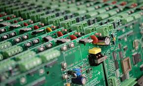
Challenges of Working With Prototype PCB Assembly
PCB fabrication is an intricate process that requires careful planning and attention to detail. Component placement is a major factor in determining how a board will be produced, and improper positioning can significantly increase the cost of your final product. Performing a DFM analysis prior to assembly can help minimize these problems.
Reworking and repairing miniaturized PCBs can be challenging, especially when the components are tightly packed together. A minor slip during rework can damage adjacent traces or components. The small space between components can also make it difficult to realign and secure mechanical joints. These problems can be further compounded by using adhesives or underfill materials to separate components.
Choosing the wrong PCB material can also be a challenge. The right material is crucial to a product’s performance, durability, and cost. Common prototype PCB materials include FR-4 (a type of fiberglass), polyimide, and metal-core PCBs for applications requiring enhanced thermal management.
Prototype PCBs are prone to a wide range of defects, including soldering defects, voids, lifted pads, webbing and splashing, tombstoning, shadowing, and more. Many of these issues can be avoided by partnering with an ECM that offers automated optical inspection (AOI). This technology uses an autonomous camera to scan and detect defects, and it can be implemented at any point during the PCB assembly process.
